Package Capability-Frontend
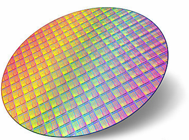
- Wafer backgrinding
- Wafer size: 8 or 12 inches
- Final thinned thickness: min 50um
- Final thinned thickness tolerance: ±10um
- Wafer sawing
- Different chunk tables with vacuum available for different wafer size
- Use DI water with CO2 and Diamaflow to avoid ESD, contamination issues
- Different blade types and optimized parameters for different wafer materials (like Si, Cmos, LiTaO3, glass)
|
|
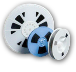
- Die to reel capacity
- Six sides inspection(missing bump, crack, breakage, contamination, etc.)
- UPH: 12~14K
- Min die size: 0.3mm*03mm
- Die material: Si, SiGe, GaAs
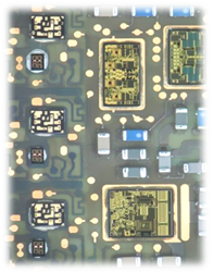
- High accuracy surface mounting technology
- Fine pitch copper pillar and CSP flip chip
- High placement accuracy(tolarance ±36um) with automatical adjustment function
- High accuracy of mounting force control
- High efficiency of fully automatic optical inspection; 100% AOI, can detect all surface defects such as missing component, tombstone, wrong polarity, shift, short, contamination, etc.
|
|
- Die attach capability
- Multiple die: multiple different dies/mutiple epoxy types
- Thin die capability
- Stack die capability
- Die attach with film
- Flip chip capability
- Solar chip capability
- High efficiency of fully automatic optical inspection; 100% AOI and it can detect all surface defects such as missing die, shift, rotation, short, epoxy on die, etc.
|
|
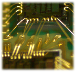
- Wire bond capability
- Wire distance: 35um
- Wire bonding accuracy: ±2um
- Cu wire and other alloy wires
- Wires on stack die capacity
- Super low loop wire capacity
- QFN capacity
- High efficiency of fully automatic optical inspection; 100% AOI and it can detect all surface defects such as missing wire,
shift, rotation, short, epoxy on die, etc.
|
|